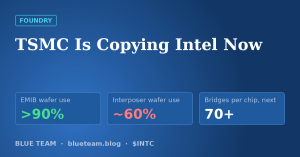
On November 4 in Busan, Intel Foundry’s packaging director Lee Kyu-oh put one number on the table that explains why the AI industry is lining up at Intel’s door. An interposer, the large slab of silicon under TSMC’s CoWoS packages, uses about 60% of a wafer. Intel’s bridge approach uses more than 90%.
That gap is the cost edge behind EMIB-T, and it is why even TSMC is now building bridges of its own.
Why the bridge wins
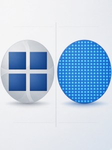
Wafers are round and interposers are big rectangles, so every interposer wafer loses its curved edges. EMIB replaces the slab with tiny silicon bridges placed only where two chips touch. They tile almost to the edge of the wafer, they need a fraction of the silicon, and a defect costs one tiny bridge instead of a whole slab.
Bernstein puts EMIB at a few hundred dollars per chip, against $900 to $1,000 for CoWoS on a Rubin-class part. Intel will price on value, not on cost, which leaves wide margins.
The roadmap is enormous
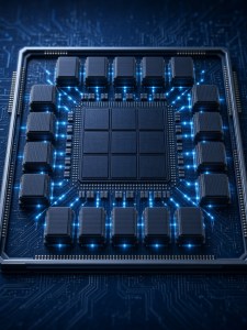
“EMIB-T provides an architecture that can flexibly respond to chip enlargement demands,” Lee said. The numbers he showed make the point.
| Stage | Package size | HBM stacks | EMIB bridges |
|---|---|---|---|
| 2026 commercial AI chips | up to 120 × 120 mm | 12 | 20+ |
| In development | 120 × 180 mm+ | 16+ | 38+ |
| Next | 240 × 240 mm | 32+ | 70+ |
The bigger AI chips get, the more an interposer costs and the wider Intel’s advantage grows. “It will become a trend to put TSVs in all bridges, considering AI chip performance,” Lee added.
The customers are real
Google has reportedly booked Intel to package more than 3 million TPUs in 2028. Amazon and MediaTek are named adopters, and MediaTek confirmed EMIB-T for its large AI chips on its own earnings call. Nvidia is reportedly evaluating Intel packaging for its 2028 Feynman chip, and SK hynix is testing its HBM on EMIB.
Even TSMC agrees

TSMC’s newest CoWoS-L already uses small local bridges inside its interposer, and TSMC is reportedly developing a fuller EMIB-like design. Its chief executive C.C. Wei has said packaging capacity limits his customers’ growth and welcomed alternatives like EMIB-T.
Intel does not need to copy CoWoS. It already offers every kind of advanced packaging: EMIB and EMIB-T bridges, Foveros and Foveros Direct 3D stacking, and its own wafers.
Made in America, today
Intel packages in New Mexico now, at Fab 9 and Fab 11X in Rio Rancho, and a new complex in Penang, Malaysia comes online in 2026. Lip-Bu Tan said on the Q3 call that Intel is adding packaging capacity in both for customer ramps next year. Intel has also locked in $5.3 to $6.1 billion of substrate supply, partly funded by customer deposits. TSMC’s first US packaging plant targets late 2027 to 2028.
The money
CFO David Zinsner has described packaging as worth several billion dollars per customer per year, at about 40% gross margin and with far less capital than a wafer fab. Customer volume production starts in 2027.
Packaging is the first part of Intel Foundry customers are paying for. Every package Intel wins brings a customer one step closer to trusting it with wafers on 18A-P and 14A.
Grogu Ledak | The Blue Team
Sources: ZDNet Korea, ISMP 2026 · Crypto Briefing · Tom’s Hardware on Google TPUs · TrendForce · Xenospectrum


Leave a Reply